Configuration Procedure for ADC, ADC_ETC, and FlexPWM Modules for Hardware-Triggered Sequence Acquisition
In the programming procedure for the ADC, ADC, ETC, and FlexPWM modules presented below, some programming examples (command lines in C language) use definitions and macros found in the imxrt.h file.
The reader should pay attention to the details of the code. It is common to use the "Read-Modify-Write" strategy using the OR operator (|=) in command lines. This allows the programmer to organize the code and act on the same register at different points, separating the bit configuration by related instances, even if they are in different registers. On the other hand, care must be taken with the reset of flags that use the "write 1 to clear" strategy, as an undesirable flag reset can occur if the OR operator is used.
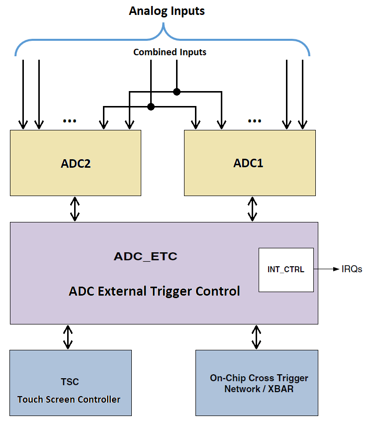
- ADC Module Configuration (both modules must be configured if applicable)
- Disable the keeper for the analog inputs to be used. In this example:
- IOMUXC_SW_PAD_CTL_PAD_GPIO_AD_B1_02 &= ~(1 << 12); // Disable Keeper for A0 (GPIO_AD_B1_02)
- IOMUXC_SW_PAD_CTL_PAD_GPIO_AD_B1_03 &= ~(1 << 12); // Disable Keeper for A1 (GPIO_AD_B1_03)
- Disable the keeper for all analog inputs used.
- In the code example shown below, only channel A0 is used.
- Enable the IPG clock for the ADC module. As an example for ADC1: CCM_CCGR1 |= CCM_CCGR1_ADC1(CCM_CCGR_ON);
- Select ADC Conversion Clock - There is a trade-off between the ADC clock frequency, which impacts conversion speed, and the accuracy of the resulting measurement. Increasing the frequency increases the conversion speed, but reduces the accuracy of the analog-to-digital conversion. Just as a reference, considering ADC clock at 20MHz, the reference voltage (VDDAD) at 3.0 V, temperature at 25°C and an average of 32 samples, a typical ENOB of 10.7 is obtained [2]. It is important to note that the maximum ADC clock frequency is 40MHz [2]. Note that in Teensy 4.1, VDDAD is connected to 3.3V. In the code examples shown below, the Asynchronous clock (ADACK = 20 MHz) is selected.
- Select high speed conversion (HSC=1). This will keep the ADACK at 20MHz. As instance, ADC1_CFG |= ADC_CFG_ADHSC;
- Make sure Low Power mode is not enabled: ADC1_CFG &= ~(ADC_CFG_ADLPC). For a given output impedance of the signal conditioning circuit, enabling Low Power mode increases the time required for proper sampling [2].
- Select the ADC resolution mode, 8, 10, or 12-bits: ADC1_CFG |= ADC_CFG_MODE(2); // MODE = 0b10 -> 12-bit conversion
- Select short sample mode for a higher sampling rate: ADC1_CFG &= ~(ADC_CFG_ADLSMP). In this case, the output impedance of the signal conditioning circuit must be low. When activated, this bit significantly increases the sampling time. This applies to signal conditioning circuits with high impedance and lower sampling rates.
- Specify the sampling time in number of ADC clock periods. In this project, 7 ADC clock periods were used: ADC1_CFG |= ADC_CFG_ADSTS(2); // Set STS=0b10 => Sample period (ADC clocks) = 7 if ADLSMP=0b => 1/20MHz*7= 350ns.
- Select trigger by hardware: ADC1_CFG |= ADC_CFG_ADTRG . This is the correct option, as ADC_ETC will send the hardware trigger signals to the ADC.
- Make sure the ADC is not in continuous conversion mode: ADC1_GC &= ~(ADC_GC_ADCO). The ADC will wait for trigger signals from ADC_ETC to perform the conversions.
- In this example, the average calculation will not be used: ADC1_GC &= ~(ADC_GC_AVGE). If it is used, configure the number of samples for the average calculation in the ADC1_CFG register, for example: ADC1_CFG |= ADC_CFG_AVGS(3);// 32 samples averaged.
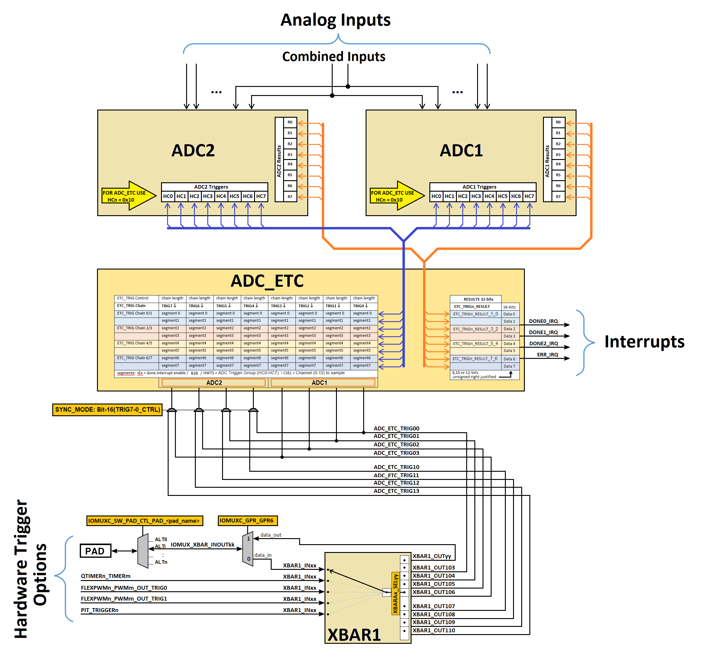
- Configure all Control registers for hardware triggers (ADCx_HCn) used in sequence configuration to 16 (0x10). This tells the ADC module that the external channel to be sampled will be selected by ADC_ETC.
- Calibrate the ADC module.
- Before the calibration process, the ADC module parameters relating to the clock source and frequency, power consumption mode, voltage reference selection, sampling time, averaging calculation, and high-speed configuration must be in accordance with the application [1].
- Ensure that the ADTRG bit is set to 0 (software trigger selected) in the ADCx_CFG register; otherwise, the calibration process will fail. Since this application refers to a hardware trigger (ADTRG=1), temporarily change the ADTRG bit to 0 until the calibration process is complete.
- To start the calibration, set the CAL bit in the ADCx_GC register.
- Wait for CAL bit becomes '0' then check the CALF (Calibration Failed Flag) status in ADCx_GS register.
- The calibration process is automatically controlled by the ADC once the CAL bit is set, and must be executed before each code operation session. The calibration result is updated internally and made available for informational purposes in the ADCx_CAL register.
- Since calibration is a process that involves triggering, waiting for completion, and verifying success, the corresponding code snippet involves a sequence of steps which, within an appropriate programming criterion, integrate more than mere lines of register configuration. Therefore, it was decided not to present individual command lines here; the reader should observe the calibration routine included in the code examples presented below.
- ADC_ETC Module Configuration
- Reset the ADC_ETC module. Since this process involves writing to the SOFTRST bit of the ADC_ETC Global Control Register and there is no way to verify if the process has completed, as is the case in the ADC calibration process, It is recommended that the CPU wait for this process to complete. See an example of how this process can be commanded in the code example below.
- In some tests performed, failures were common at the beginning of the ADC1-ADC_ETC communication. Therefore, as a precaution, as can be seen in the example code, the ADC_coco flags (conversion complete flags) were reset at this point by reading all the result registers of ADC1. This is a sort of ADC1 reset.
- According to the chosen ADCT_ETC trigger, specify in the respective TRIGx_CTRL register the number of channels to be sampled in the sequence. TRIG_CHAIN = n implies (n+1) channels. In this presentation, the ADC_ETC trigger0 will be used with a sequence composed of 4 channels: ADC_ETC_TRIG0_CTRL = (ADC_ETC_TRIG_CTRL_TRIG_CHAIN(3)).
- Configure the sequence or sequences if more than one ADC_ETC trigger is used. This presentation shows the configuration of only one sequence for ADC_ETC Trigger0. The sequence for the ADC_ETC trigger0 is specified in the ADC_ETC_TRIG0_CHAIN_x_y registers, two channels per register. For a 4-channel sequence, we have:
- ADC_ETC_TRIG0_CHAIN_1_0 =
| ADC_ETC_TRIG_CHAIN_HWTS0(1 << 0) | | // LOWER WORD: Target ADC1 Slot 0 (HC0) for first sample |
| ADC_ETC_TRIG_CHAIN_CSEL0(A0) | | // Sample A0 (A0 is a macro name defined before - Hardware Channel 7) |
| ADC_ETC_TRIG_CHAIN_IE0(0) | | // No interrupt after first sample |
| | |
| ADC_ETC_TRIG_CHAIN_B2B1 | | // Start this second conversion immediately after adc_coco (conversion complete flag) from first conversion |
| ADC_ETC_TRIG_CHAIN_HWTS1(1 << 1) | | // UPPER WORD: Target ADC1 Slot 1 (HC1) for second sample |
| ADC_ETC_TRIG_CHAIN_CSEL1(A1) | | // Sample A1 (A1 is a macro name defined before - Hardware Channel 8) |
| ADC_ETC_TRIG_CHAIN_IE1(0)) | ; // No interrupt after second sample |
-
- ADC_ETC_TRIG0_CHAIN_3_2 =
| ADC_ETC_TRIG_CHAIN_B2B0 | | // Start this third conversion immediately after adc_coco (conversion complete flag) from second conversion |
| ADC_ETC_TRIG_CHAIN_HWTS0(1 << 2) | | // LOWER WORD: Target ADC1 Slot 2 (HC2) for third sample |
| ADC_ETC_TRIG_CHAIN_CSEL0(A2) | | // Sample A2 (A2 is a macro name defined before - Hardware Channel 12) |
| ADC_ETC_TRIG_CHAIN_IE0(0) | | // No interrupt after third sample |
| | |
| ADC_ETC_TRIG_CHAIN_B2B1 | | // Start this fourth conversion immediately after adc_coco (conversion complete flag) from third conversion |
| ADC_ETC_TRIG_CHAIN_HWTS1(1 << 3) | | // LOWER WORD: Target ADC1 Slot 3 (HC3) for fourth sample |
| ADC_ETC_TRIG_CHAIN_CSEL1(A3) | | // Sample A3 (A3 is a macro name defined before - Hardware Channel 11) |
| ADC_ETC_TRIG_CHAIN_IE1(1) | ; // Interrupt (Done0) at the end of fourth sample |
- Some information regarding the presented sequence configuration is important:
- Triggers 0, 1, 2, and 3 internal to the ADC were used; that is, slots 0, 1, 3, and 3 were programmed in the HWTS (ADC hardware trigger selection) bits of the sequence configuration registers. This means that the corresponding ADC_HCn registers internal to the ADC must be configured to 0x10. It is possible to reuse the same trigger, so the same slot could be used for the entire sequence.
- As soon as the ADC receives the first trigger from the ADC_ETC, it initiates the sampling and conversion process of the first channel in the sequence. However, for the remaining channels in the sequence, it is important to specify the B2B bit (Back to Back ADC trigger) in the ADC_ETC_TRIG0_CHAIN_x_y register. Normally, B2B=1 is used; that is, as soon as the ADC_ETC receives the ADCxCOCOn signal (Conversion Complete Flags in ADCx_HS), it sends the trigger signal for the next conversion. If B2B=0 is configured, the ADC_ETC will not wait for the conversion complete signal; it will send the trigger for the next acquisition as soon as the sample interval expires. Therefore, the sample interval must necessarily be configured in the ETC_TRIGx Counter Register (in this example, ADC_ETC_TRIG0_COUNTER). The default value for the sample interval time is zero, so if B2B=0, the next trigger will be sent immediately after the current trigger and the current acquisition will not be performed (result register = 0x0000). Note that a sample interval time greater than the time required for sampling and conversion must be specified. In this presentation, B2B = 1 was configured, as this option is recommended for the fastest execution of the acquisition sequence.
- According to [1], page 3414, the total conversion time will be Conversion_Time = SFCAdder + Average_Num*(BCT+LSTAdder):
- In this presentation ADC_CLK = ADACK (20MHz) and Average_Num = 1:
- SFCAdder = 3 ADCK cycles (before starting of conversion) + 1 ADCK (after end of conversion) + 2 bus clock cycles, thus SFCAdder = 3/20MHz + 1/20MHz + 2/150MHz
- BCT (12-bits) = 25 ADCK cycles = 25/20MHz
- LSTAdder (ADLSMP=0; ADSTS=10) = 7 ADCK cycles = 7/20MHz
- Thus total conversion time is 1.8133e-06 s.
- If the programmer decides to set B2B=0, then the sampling time interval must be specified in the ADC_ETC_TRIG0_COUNTER register (trigger0 used in this example). The pre-divider value must also be defined in the ADC_ETC_CTRL register. At this point, there seems to be a trick not revealed in the manual, as the specifications don't seem to have the desired effect for pre-divider=0, but for values equal to or greater than 1 applied to the example code below, they result in the correct acquisition of the sequence. Considering an acquisition time of 1.8133e-06 s and a pre-divider of 1, this will result in a sample interval greater than 135 (1.8133e-06*150e6/2-1).
- In the example given, the `done0` interrupt was configured at the end of the sequence. It is possible, for example, to configure up to 3 sequences with distinct interrupts (`done0`, `done1`, and `done2`). From there, the IRQs must be shared, requiring verification of the respective flag within the ISR for proper data handling.
- An interrupt can be specified before the end of the sequence, but this is not usual, since the respective ISR would have very little time to process anything and could delay the execution of the end-of-sequence interrupt, in the case of using a different IRQ, or it could generate problems identifying the order of calls to the same IRQ. Typically, a single interrupt is enabled at the end of the sequence.
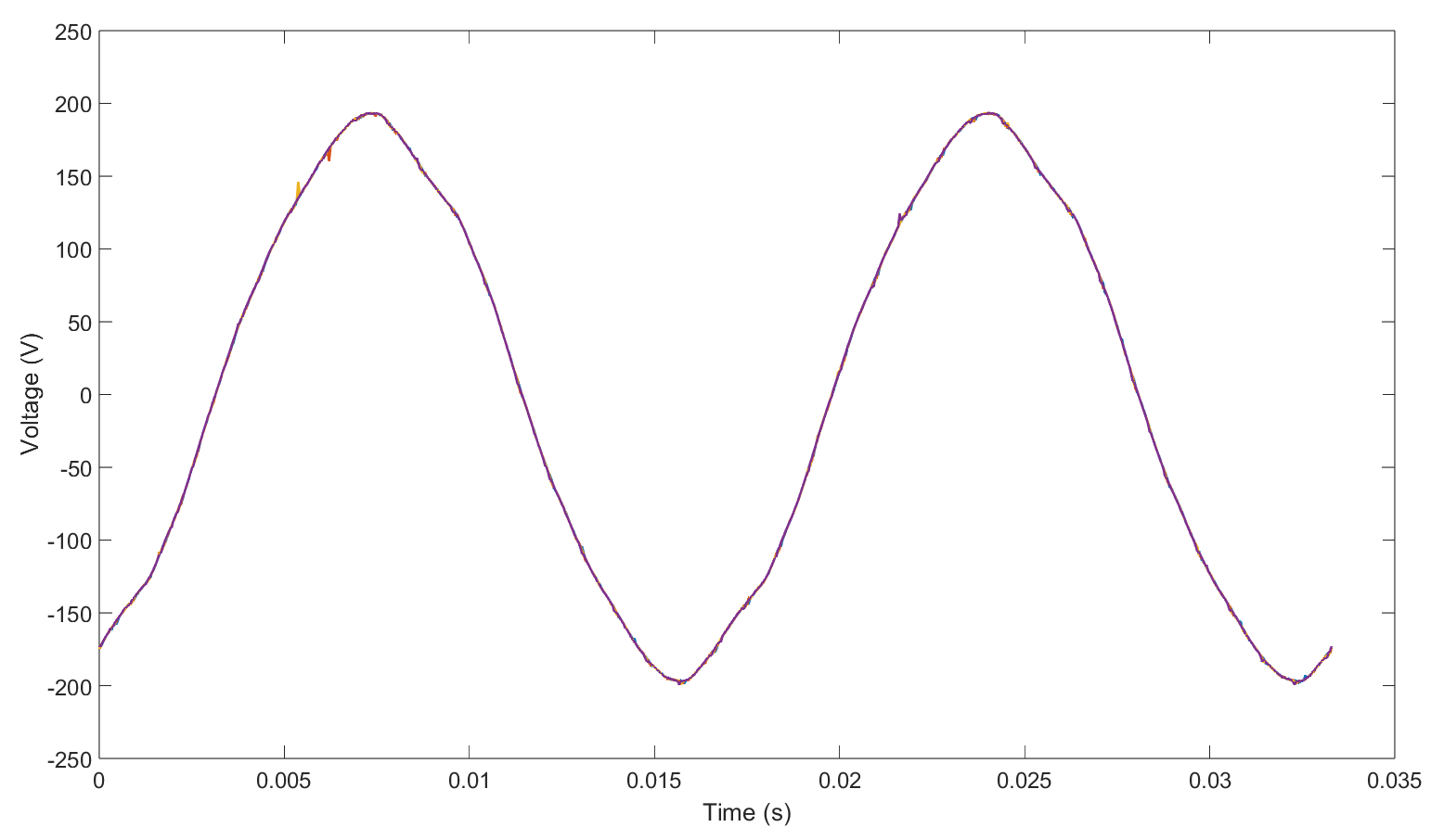
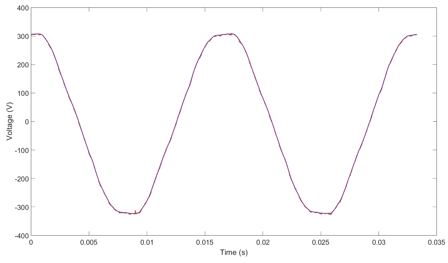
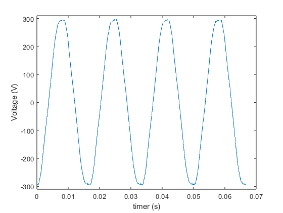
- It is possible to specify any channels in any order in the list of channels that make up the sequence, including repeating channels. In the results presented below, to reduce the laboratory resources used in the test, only one voltage sensor and its respective signal conditioning circuit were used in the lab, connected to channel A0. Thus, the channel list consisted of 4 sequential readings from channel A0.
- Install the ISR for end of sequence and enable the corresponding IRQ flag in NVIC. In this example, the done0 interrupt was used.
- attachInterruptVector(IRQ_ADC_ETC0, &adc_etc_done0_isr);
- NVIC_SET_PRIORITY(IRQ_ADC_ETC0, 0x80); //medium priority level - Level 8 out of 15 (16 levels)
- NVIC_ENABLE_IRQ(IRQ_ADC_ETC0);
- Install the ISR for ADC_ETC error handling and enable the corresponding IRQ flag in NVIC.
- attachInterruptVector(IRQ_ADC_ETC_ERR, &adc_etc_error_isr);
- NVIC_SET_PRIORITY(IRQ_ADC_ETC_ERR, 0x90);
- NVIC_ENABLE_IRQ(IRQ_ADC_ETC_ERR); //Level 9 out of 15 (16 levels)
- Note: Within the ISR related to the ADC_ECT error interrupt, in addition to resetting the interrupt flag and signaling the main code of the existence of an error situation, modifying a variable, read all internal result registers ADCx_Rn to reset the ADCx_coco flags (conversion complete flags).
- Enable the trigger and triggers to be used by ADC_ECT in the ADC_ETC_CTRL register. In the example adopted, only trigger0 will be enabled: ADC_ETC_CTRL |= ADC_ETC_CTRL_TRIG_ENABLE(1 << 0).
- XBAR1 Module Configuration
- Enable Clock for XBARA1: CCM_CCGR2 |= CCM_CCGR2_XBAR1(CCM_CCGR_ON).
- Route the trigger connection on XBAR1. In the example adopted in this presentation, the trigger signals FlexPWM4_SM2_TRIG0 OR FLEXPWM4_PWM2_OUT_TRIG1 (XBAR1_IN54) will be routed to ADC_ETC_TRIG00 (XBAR1_OUT103). Thus, in the input selection register for output XBAR1_OUT103 select XBAR1_IN54: XBAR1_SEL51 |= (54 << 8). Note that the selection field of interest is in the upper byte. As mentioned earlier, such trigger signals are incorrectly listed for input XBAR1_IN53, Table 4-5. - XBAR1 Input Assignments, page 62 of [1].
- FlexPWM Module Configuration
- Configure a FlexPWM PWM module to generate trigger signals according to the application. It is common in power electronics converter control applications to use a FlexPWM module to control the power flow to the converter output and synchronously trigger the acquisition system to read the variables to be fed back. Since there is a huge range of applications, this presentation will focus only on the important details for generating the trigger signal. More details can be found at How to Configure FlexPWM on Teensy 4.1
- Enable Clock for FlexPWM Module. In this example the FlexPWM4 is used: CCM_CCGR4 |= CCM_CCGR4_PWM4(CCM_CCGR_ON).
- Select FlexPWM clock source. In this example, the IPG clock (150MHz) is selected for submodule 2 of FlexpWM 4: FLEXPWM4_SM2CTRL2 = FLEXPWM_SMCTRL2_CLK_SEL(0).
- Define the prescale (division factor for the clock). In this example, divide by 1: FLEXPWM4_SM2CTRL = FLEXPWM_SMCTRL_PRSC(0)
- Define counter range:
- Following the example presented in How to Configure FlexPWM on Teensy 4.1, and considering TOP=6250, we will have a carrier frequency equal to 12kHz:
- FLEXPWM4_SM2INIT = -TOP; // Carrier BOTTOM
- FLEXPWM4_SM2VAL0 = 0;
- FLEXPWM4_SM2VAL1 = TOP-1 //Carrier TOP - For TOP= 6250 => Freq_carrier = IPG_CLk/prescaler/counting steps => 150MHz/1/(2*6250)= 12kHz
- Enable the FlexPWM trigger(s) as desired for the application. In this example, both triggers will be enabled: FlexPWM4-SM2 trigger0 and FlexPWM4-SM2 trigger1:
- FLEXPWM4_SM2TCTRL |= (FLEXPWM_SMTCTRL_OUT_TRIG_EN(1 << 0) | FLEXPWM_SMTCTRL_OUT_TRIG_EN(1 << 1));
- Note: As can be seen on page 3169 of [1], FlexPWMnSMm_TRIG0 and FlexPWMnSMm_TRIG1 can be activated at specific points within the PWM cycle, determined by the VALk comparison registers. In the example shown, trigger0 was selected when the counter matches the value in VALO (half cycle) and trigger1 when the counter matches the value in VAL1 (full cycle). This represents two samples per PWM cycle, implying a sampling frequency (24kHz) twice the carrier frequency (12kHz).
- Whenever the comparison registers (VALk) are changed, remember to load them, as the comparison registers are buffered and will only take effect after LDOK is activated to load the values internally into the PWM generating unit.
In this example: FLEXPWM4_MCTRL |= FLEXPWM_MCTRL_LDOK(1 << 2).
- Start the counter for the internal FlexPWM submodule being used. In this example: FLEXPWM4_MCTRL |= FLEXPWM_MCTRL_RUN(1 << 2);
- Notes:
- The steps above constitute the minimum configurations for generating a trigger corresponding to double sampling per PWM cycle. Further configurations will depend on the application.
- In the code examples shown below, for illustrative purposes only, in addition to generating a trigger for the ADC_ETC, a sinusoidal pulse width modulation was generated at the PWMA output of submodule 2 of the FLEXPWM 4 module (PWMB will be a complementary signal of PWMA).
References
[1] i.MX RT1060 Processor Reference Manual, Rev. 3, 07/2021, NXP Semiconductors.
[2] i.MX RT1060 Crossover Processors for Consumer Products, Rev. 4, 04/2024, NXP Semiconductors.
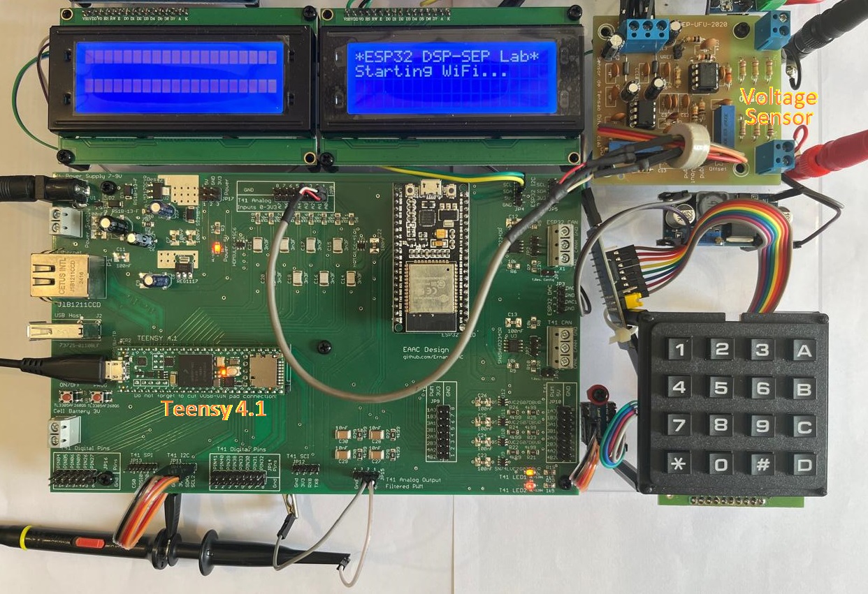
[3] PJRC Electronics Projects - Teensy® 4.1 Development Board